Silicon nozzle technology
Realizing high accuracy of dot placement and a wide media gap by nozzle hole forming technology using MEMS
\Our expert team handles inquiries
on technical partnerships and joint research./
Highly dot placement accuracy and a wide media gap for an increased range of printing applications involving three-dimensional objects
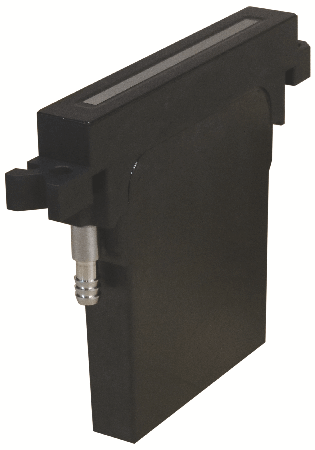
Display and printed circuit board manufacturing processes use inkjet printing and require exceptionally high precision of dot placement. Moreover, inkjet printing is increasingly used in printing on three-dimensional objects such as tubes and containers (direct-to-shape [DTS] printing). For printing on three-dimensional objects, the distance between the head and the printed object (media gap) needs to be enlarged because the surfaces of such objects are not flat. Konica Minolta’s inkjet heads have been widely adopted for DTS applications due to the slimness of the head. Silicon nozzle technology increases dot placement accuracy compared with previous head models and will further extend the range of applications.
Technology Overview
Silicon nozzle technology forms head nozzle holes by using a processing technique known as the microelectromechanical systems (MEMS) process. The MEMS process, which is based on semiconductor manufacturing processes, is used to construct three-dimensional structures on a silicon substrate or other material. Silicon nozzle technology ensures higher processing accuracy than is possible with the conventional technology of using laser machining to form nozzle holes in polyimide sheets. The head jets ink droplets with higher directional accuracy with increasing nozzle positioning accuracy. The jetting straightness of ink droplets is improved with higher circularity of the nozzle hole. Consequently, the use of silicon nozzle technology ensures higher directional accuracy and a wider media gap than previous nozzle models.
\Our expert team handles inquiries
on technical partnerships and joint research./